「7nmの半導体」に7nmの箇所はどこにもなかった
(写真はイメージ)
(画像1/6)
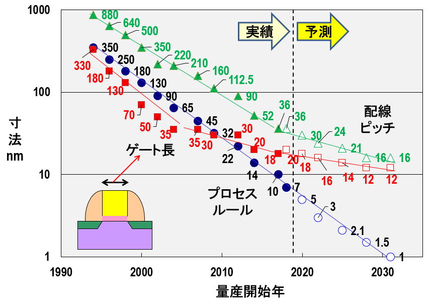
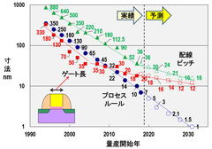
図1 半導体微細化の推移と将来予測
出所:平本俊郎(東京大学生産技術研究所)『日経新聞「経済教室」』(7月18日)
出所:平本俊郎(東京大学生産技術研究所)『日経新聞「経済教室」』(7月18日)
(画像2/6)
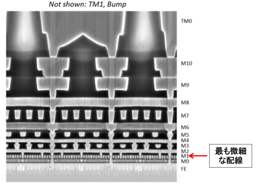
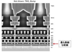
図2 インテルの10nmチップの断面SEM写真
出所:インテル、IEDM2017-674
出所:インテル、IEDM2017-674
(画像3/6)
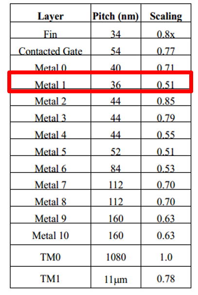
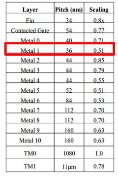
図3 インテルの10nmチップの配線ピッチとスケーリング
出所:インテル、IEDM2017-674
出所:インテル、IEDM2017-674
(画像4/6)
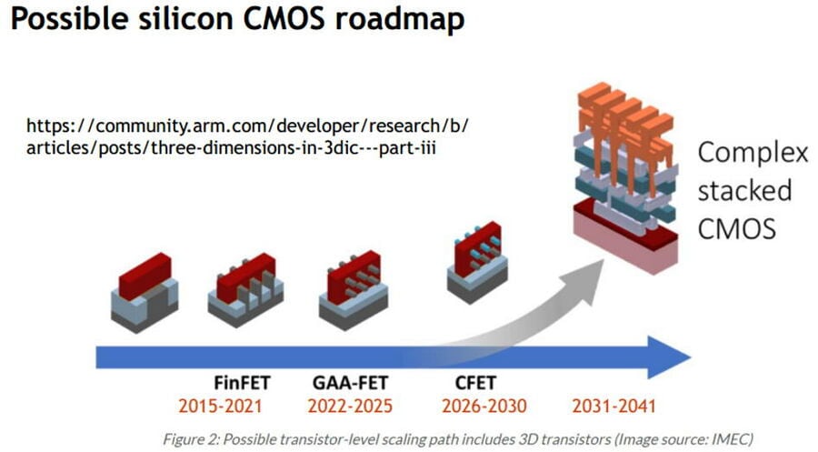
図4 3次元化するトランジスタ構造
出所:B. Cline and D. Prasad, Arm Ltd.., “DTCO in 2019: The Precious Metal Stack and the Route to Better Designs”, Short Course 1, VLSI2019より
出所:B. Cline and D. Prasad, Arm Ltd.., “DTCO in 2019: The Precious Metal Stack and the Route to Better Designs”, Short Course 1, VLSI2019より
(画像5/6)
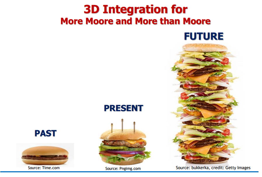
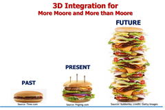
図5 3次元方向にチップを積層すれば集積度が上がる!
出所:C. H. Tung, TSMC, “3D Integration for More-Moore and More-than”, Short Course 1, VLSI2019より
出所:C. H. Tung, TSMC, “3D Integration for More-Moore and More-than”, Short Course 1, VLSI2019より
(画像6/6)


「7nmの半導体」に7nmの箇所はどこにもなかった
この写真の記事を読む